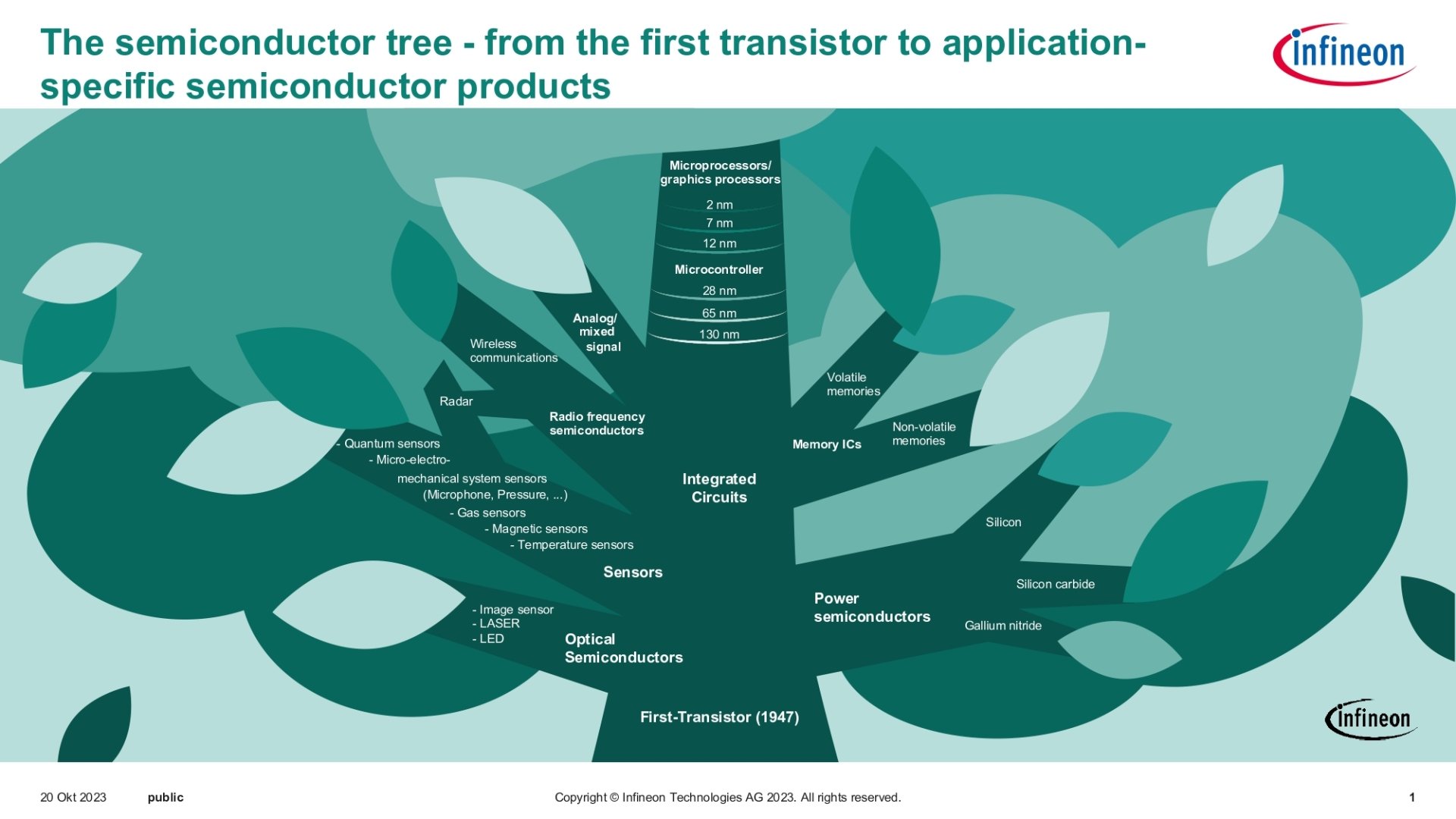
The term “legacy semiconductor” encompasses a broad range of technologies that vary greatly in their specialization, build, and price. The average smartphone has more than a thousand semiconductors, each of which costs just cents to make, while highly specialized nodes, like the radiation-hardened semiconductors used in airplanes and satellites, are thousands of dollars. Across all applications for legacy semiconductors, the Honorable Nazak Nikakhtar, former assistant secretary for Industry and Analysis at the Department of Commerce and partner at Wiley Law, noted that these chips make up 95% of the commercial market. Beyond their economic importance, legacy chips also impact national security; “of the Department of Defense’s national security, mission-critical, pentagon-style capabilities, about 99.5% depend on legacy chips,” reported Nikakhtar. While labels like “legacy” and “mature” suggest that advanced semiconductors are past their prime, their pervasiveness as commodities and in national security capabilities prove their enduring importance.
The Most Complex Facilities in the World
Building domestic manufacturing capacity for semiconductors is a key goal of the CHIPS Act, one that comes with a number of challenges. Mark Garvey, president of Global Business Unit for Advanced Technology Facilities at Exyte Asia-Pacific, explained that semiconductor fabrication plants, called fabs, “are basically the most sophisticated facilities on the planet” because of all the gases, chemicals, and controlled environments required in the manufacturing process. A large proportion of semiconductors used in the United States are manufactured overseas, especially in countries like China, Taiwan, and Singapore. According to Garvey, timelines for permitting a fab in the East are roughly half of what they are in the West. Garvey accounted for this by pointing out that in Asia, “governments actively support the permitting process to be a green lane functionality. They want to facilitate the investment.” He also noted that the familiarity these governments have with the permitting process for fabs is an advantage over the West. Lack of familiarity, combined with rightful caution concerning the potentially dangerous chemicals fabs handle, can greatly delay the permitting process.
Once permits are complete, it is time to build the fab. Like permitting, timelines for fab construction in Asia are more compressed. Garvey revealed that it takes 26 months to go from the first concrete pour to a finished clean room in the United States, while the same process takes just 12-13 months in Taiwan. Additionally, Garvey shared that the scale of fabs has grown to almost three times what it was just 15 years ago, and at the peak of manpower demand, 5,000-7,000 workers are needed during construction. Again, many Asian countries have an advantage due to more relaxed labor laws and greater labor availability. Though the CHIPS Act allocates billions of dollars to incentivize reshoring semiconductor manufacturing, boosting domestic capacity requires policymakers to address the many challenges in permitting and constructing fabs in the United States.
Short-Term Pain, Long-Term Gain
The market for semiconductors is growing each year, and while the relative shares held by the United States and its allies are declining, China’s stake continues to grow.


